
Design Tools
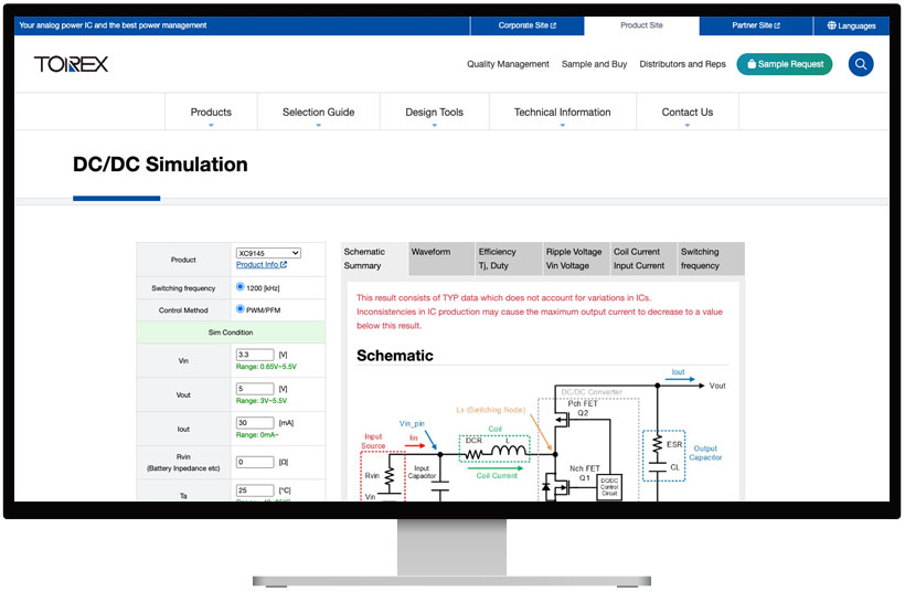
DC/DC Simulation
This tool simulate operation of the DC/DC converter,Provide design information for the selection of IC or peripheral components and circuit feasibility.
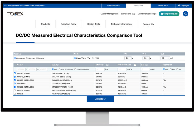
DC/DC Measured Electrical Characteristics Comparison Tool
Actual measurement data of DC/DC converter efficiency, ripple voltage, output voltage (load regulation), etc., and mounting area including peripheral components can be compared.
SPICE Model
Download Spice Model. Operation confirmed with Pspice Ver.16.3, Ta=25℃ compatible model.